Dumping a SLC NAND Flash with Atmel PMECC
Dumping a NAND flash memory can be tricky. Especially with proprietary ECC. Here we dump an SLC NAND flash with PMECC correction.
Introduction
I love to reverse engineer many things I can access to and learn from the ingeniosity of engineers who worked on the things I study. In this one I was surprised because this was my first hardware reverse engineering experience and the vendor had done a pretty neat job securing it.
I had to desolder the NAND Flash memory and do a bare read on it. I first thought that once I had my NAND Flash dump it would be easy to recover the firmware. I was wrong, and I struggled several weeks to recover data, Error Code Correction (ECC) bytes and to understand the ECC used to correct bytes (I really needed it).
After struggling several weeks with this, I finally obtained valid data decoding the PMECC codes left by the processor in the spare areas of my chip. Because the PMECC mechanism lacks online documentation allowing to reimplement it in software, this post is like a memo for me if encounter this situation again and a technical description on the dumping process for anyone interested.
The desoldering and the dumping
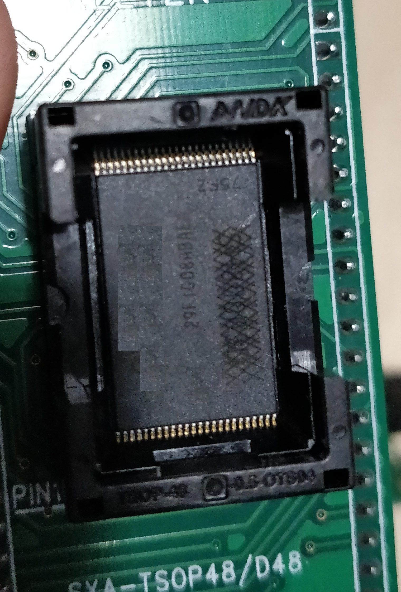
On the PCB, my NAND Flash was a TSOP48 chip :
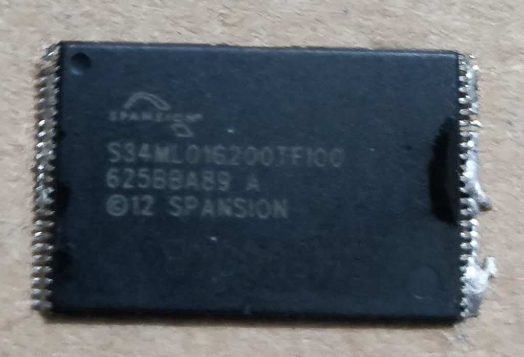
On the above picture, you can see that I used the well-known brutal desoldering using way too much solder to dissolve the flux. Obviously I took nearly 2 hours to clean the mess trying to not destroy one of the 48 0.5mm pins (and the chip because of heat). I didn’t fully succeed because pin 1 betrayed me and broke. But this is not a problem as the datasheet says that it is not used.
There are cleaner ways when you have the appropriate equipment and I will let Qwant tell it for you here.
Note : I enventually bought the proper equipment and this is way better… If you don’t burn the chip by not correctly mounting it on your adapter, I’m a moron.
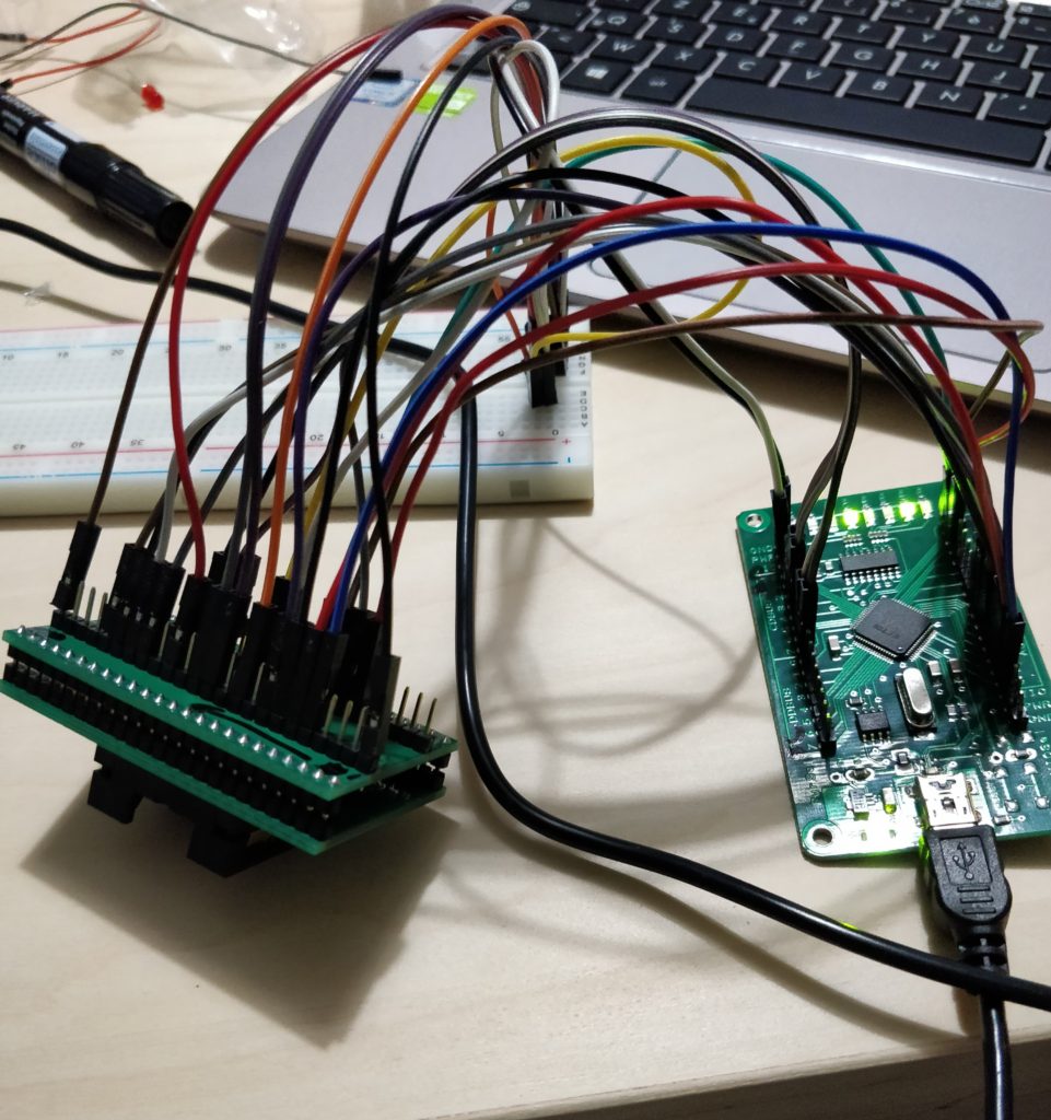
I planned this desoldering as my last chance (yes a board with no root console on UART, no open JTAG, mutual authentication for each data stream on the network, …) and got myself an FTDI FT2232H breakout board on Aliexpress because some people way more clever than me used it for this purpose and developped the appropriate software : SpriteMods and Oh Jeong Wook. If you read this, thank you guys, your researches saved my wallet and my project.
Note 1 :
Check, double check, triple check before you power on your reader. Like I said I broke pin 1 and I then though pin 2 was pin 1 (I didn’t see it at first). This is a miracle that the whole thing didn’t blow up to my face… At least my FTDI board had some nice LED blinking (LEDs not supposed to blink).
Note 2 :
If your documentation or tutorial names different buses than the ones you have on your board (like when the latter is chinese), take the FTDI datasheet and trace the pins. This could help to get the right pins at the right place. And beware : BDBUS is maybe not what the PCB says…
When the NAND contents were dumped I though I won. But this is too easy, right ?
Spaghettis someone ?
F****** errors
I learned the hard way that NAND Flash are not what I would qualify as perfectly reliable memory technology. But it is cheap, right.
Note :
Here I’m a bit cynical. In fact, NAND Flash have some advantages that makes them good ROM supports :
- They tolerate brutal power cuts
- They tolerate shocks
- They have a data retention of 10 years if the blocks are not reprogrammed beyond the manufacturer’s limit
First of all, I learned that NAND Flash memories degrade with writes. When you write a block (which is not a page, or a sector which got me confused because I didn’t know how it works) many times you have a chance to break it at last and turn it into an unusable soup of bits. Even worse : some blocks are already bad at the exit of the factory. But you know, it’s cheap.
Fortunately, the vendor marks bad blocks into a special area of some pages of the blocks affected. I learned how it works with the datasheet obtained by typing the chip reference in my favorite search engine. In my case, this marker is integrated in the first byte of the magical spare area of the first, the second or the last page of the block. If none of these bytes is set to 0xFF, the block is bad.
Oh by the way in my case pages are 2048-byte long, spare area is a 64-byte long space after each page and a block is 64 pages. A standard, the ONFI interface, allows to query the chip to know its capabilities and properties.
So when I identified bad blocks I was like “now I only have good blocks, give me my precious data”. But no, this is still too simple pal, look I inverted some bits for you. Oh just one out of 128 bytes in your fabulous good blocks.
And this is why NAND Flash controllers implement a Error Correcting Code when managing such devices. So the board I was analyzing had an AT91SAMA5D31 SoC as main CPU. This model (according to the datasheet) accelerates ECC with an hardware implementation of the BCH algorithm.
As some people already tried on the Internet, without success, I also tried to naively decode the ECC bytes using the bch.c code written for the Linux kernel. I had no success in this task at first. Doubting of my parameters, I read again Atmel’s datasheet and found that at address 0x0 of the NAND Flash there was a configuration header repeated 52 times (repeated because at this stade no ECC can correct it).
This header had the following specification :
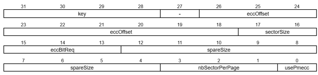
ECC Header as described in AT91SAMAD3 series datasheet
Two things :
- The processor is reading this in little endian (not surprising)
- It reverses the bits order when reading each byte!
As an exercise, I manually interpreted the following header I saw in my dump :
Original 05 24 90 c0
Transcripted in binary (and reversed endianness to better reading): 1100 0000 1001 0000 0010 0100 0000 0101
eccOffset = 36
sectorSize = 0 (512)
eccBitReq = 1 (4 bytes)
spareSize = 64
nbSectorPerPage = 2 (this doesn't seem to be respected by the PMECC engine)
usePmecc = True
Cool, I have the configuration of the PMECC engine integrated in the processor.
I applied the same principle to the data and ECC code I was retrieving. And voilà, I managed to correct a significant amount of sectors (something like 80 000 correctable vs 50 000 uncorrectable sectors and a bit over 30 000 of blank sectors)! But I still had also a huge amount of errors because of some alien signal disturbing my data transfer moron who doesn’t know how to read a datasheet.
You’ll find here a (quick and dirty !) Python code correcting errors with PMECC. It requires python-bchlib and Python 3.5 to work (python-bchlib requires it). You have to feed it the raw NAND dump with spare areas after each page. The script will try to deduce configuration from the PMECC header if present.
Download it here : PMECC reader and decoder
Note : this script is under the WTFPL license.
Some limitations of this script :
- It’s dirty and really not optimised
- It does not natively support other than 7-byte ECC code (this should be fine for the majority of applications)
Functionnalities :
- It can combine several dumps of the same chip, taking the first sector which can be corrected by ECC in the several files given
- It works fine in a few minutes for 3 or 4 dumps of ~130MB
Wear leveling and very special filesystems
As I said earlier, the blocks in a NAND flash have a limited supported erase/program cycle number. So to balance the writing load on the memory chip, a process known as wear leveling is used. In my case, this is implemented at software level in the Linux kernel.
The modern technique, implemented in my case, is the UBI (Unsorted Block Image) volume management system. This system adds information to each block that includes volume number, erase cycle number of the block or the Logical Erase Block correspondance with Physical Erase Block.
To achieve the wear leveling, the UBI system maps LEB to PEB in order to allow relocation of LEB on another physical block in the event of a write operation. Each of these blocks can then be attached to a particular volume containing a filesystem.
But it is impossible to use classical filesystems in this case because Flash Memory are not a classical block device. And in fact, USB sticks and SD cards trick the OS into making it think they are block devices with a dedicated microcontroller on the chip. This is not the case here and I observed 4 types of (not always) filesystem in my case :
- Linux zImage (for booting the whole thing obviously),
- DTB volume (Device Tree Binary to tell the OS how to handle the hardware),
- Squashfs (Static content used by the OS to get customer specific configuration data),
- UBIFS (for all dynamic and static FS accessed by the OS).
As it name suggests, UBIFS is a filesystem concious of the UBI constraints which copes with the NAND Flash problems aswell as brutal poweroff or integrity checks (but not correction).
I will certainly write more about that later.
Conclusion
The project that headed me to this mess is still not finished. But I’m glad I could overcome some of the most serious obstacles with the help of some people in the community. I now feel like that the most difficult is behind me, I just have to buy a new box (you know the thing I’m trying to understand) and read that famous filesystem (my tests on this bogous copy were encouraging).
It never ceases to amaze me how much clever solutions are put into a thing as basic as a NAND Flash chip that we produce by billions and use everyday.